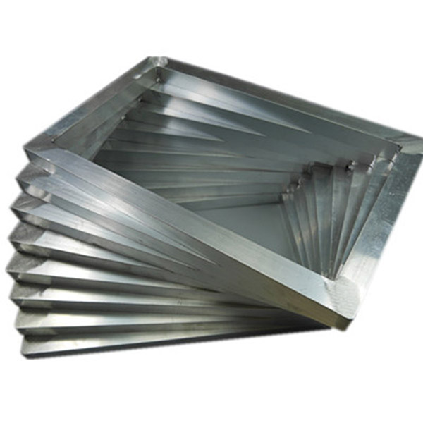
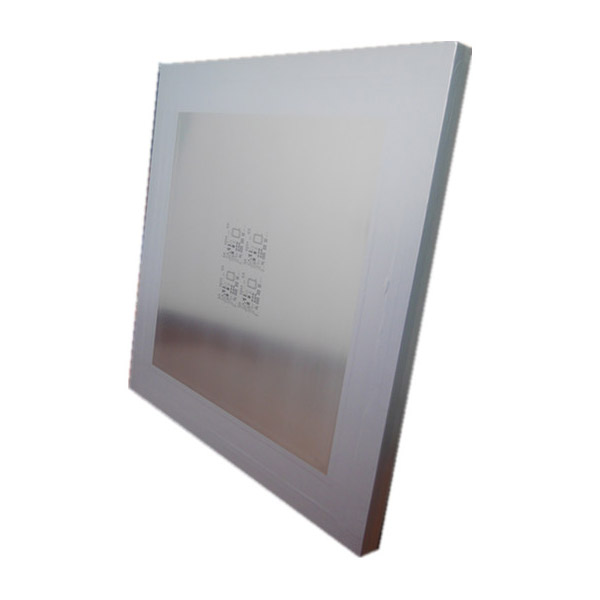
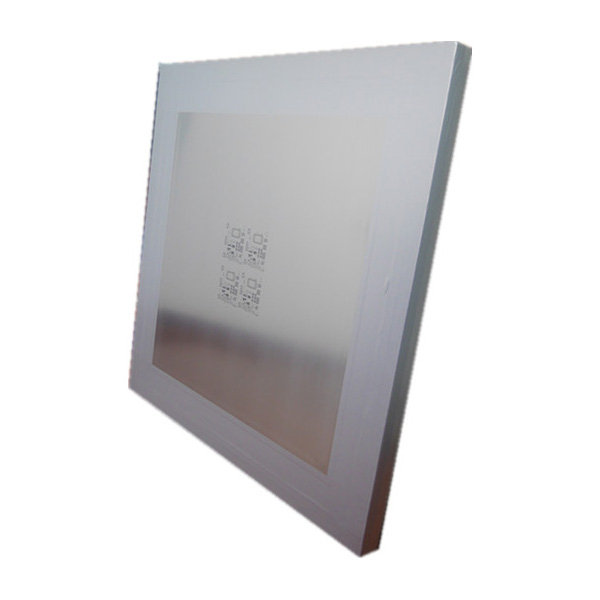
In terms of the production process, it can be approximately divided into laser stencil, electropolished stencil, nano stencil, electroformed stencil, etched stencil, step stencil, etc.
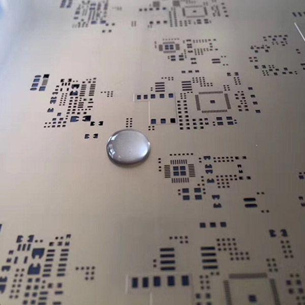
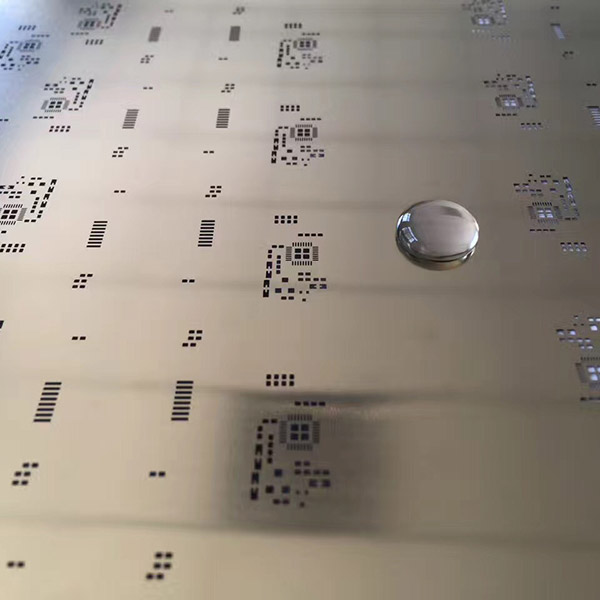
1) Laser stencil is cut and shaped by laser, which is the most common stencil in the industry at present. It is made directly by the data file, which reduces the production error link and has high precision, but it needs to be cut one by one and is not fast.
2) Electro-polished stencil is polished and polished the whole wall of the stencil by electrolytic polishing after laser cutting to improve the open hole wall. Its hole wall is smooth and especially suitable for ultra-fine pitch QFN/BGA.
3) Nano stencil is based on the electro-polished stencil with some nano rare metals added on its surface, and by changing the metal structure to make it well bonded, the hardness of the stencil is greatly improved and the rare metals have a repulsive effect on the flux in the solder paste, thus greatly reducing the number of screen washing and improving the production efficiency and printing quality. Nano stencil has all the advantages of the electropolished stencil, its non-stick paste advantages make its printing
more difficult to pull the tip, suitable for more precise components of the solder paste printing.
4) Electroforming stencil is the most complex type of stencil manufacturing technology, a metal forming process that forms a metal layer by depositing nickel metal onto a base plate or stencil. Electroforming stencil has smooth hole wall, inverted trapezoidal structure, best solder paste release, good printing performance for micro BGA, ultra-fine pitch QFP, and small chip components such as 0201, 01005. And because of the characteristics of the electroforming process itself, the edge of the hole to form a slightly higher than the thickness of the stencil ring protrusion, solder paste printing is quite a "sealing ring", in the printing of this sealing ring is conducive to stencil and pad or solder resist film close fit, to prevent the leakage of solder paste to the outside of the pad. Of course, the cost of this process stencil is also the highest.
5) Etched stencil is through the chemical etching process, once formed, faster, in the laser stencil is not popular when the mainstream stencil, with the development of technology and the increasing requirements for environmental protection, the etched stencil has been replaced by laser stencil, but the etching process as still irreplaceable.
6) Step stencil: step stencil is made of two or more thicknesses on the same stencil to achieve accurate control of the amount of tin, STEP-UP local thickening can overcome the problem of uneven foot position of some parts, while STEP-DOWN local thinning stencil can effectively control the FINE PICTH parts foot short circuit problem.